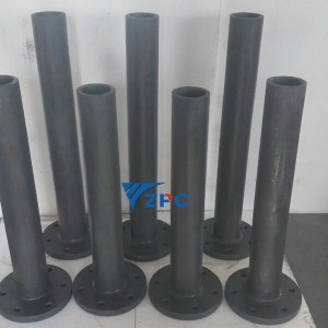
SiC substrate mo le ufiufiina o le ata tifaga CVD
Fa'aputuga o le Ausa Fa'akemikolo
O le chemical vapor deposition (CVD) oxide o se faagasologa tuputupu aʻe laina lea e faʻapipiʻi ai e se kasa muamua se ata manifinifi i luga o se wafer i totonu o se reactor. O le faagasologa tuputupu aʻe e maualalo le vevela ma e maualuga tele le fua faatatau o le tuputupu aʻe pe a faʻatusatusa i leokisa vevela. E maua ai fo'i ni vaega manifinifi o le silicon dioxide auā e fa'aputuina le ata tifaga, nai lo le fa'atupuina. O lenei faiga e maua ai se ata tifaga e maualuga lona tete'e atu i le eletise, lea e sili ona lelei mo le fa'aaogaina i ICs ma masini MEMS, fa'atasi ai ma le tele o isi fa'aoga.
E faia le chemical vapor deposition (CVD) oxide pe a manaʻomia se vaega i fafo ae atonu e le mafai ona faʻaʻokeseneina le silicon substrate.
Tuputupu aʻe o le Faʻaputuina o le Ausa Kemikolo:
E tupu le tuputupu aʻe o le CVD pe a faʻaofiina se kesi poʻo se ausa (precursor) i totonu o se reactor e maualalo le vevela lea e faʻatulaga ai wafers i luga pe faʻalava. E fealuaʻi le kesi i totonu o le faiga ma tufatufa tutusa i luga o le fogāeleele o wafers. A o fealuaʻi nei precursors i totonu o le reactor, e amata ona mitiia e wafers i luga o latou fogāeleele.
O le taimi lava e salalau tutusa ai mea muamua i totonu o le faiga, e amata loa ni tali fa'akemikolo i luga o le fogāeleele o mea e fa'apipi'i i ai. O nei tali fa'akemikolo e amata o ni motu, ma a'o fa'aauau pea le faiga, e tuputupu a'e motu ma tu'ufa'atasia e fausia ai le ata tifaga e mana'omia. O tali fa'akemikolo e fausia ai ni mea e lua i luga o le fogāeleele o le pa'u, lea e sosolo atu i le vaega tuaoi ma tafe atu i fafo o le reactor, ma tu'ua ai na'o pa'u ma lo latou ata tifaga ua fa'aputuina.
Ata 1

Aogā o le Fa'aputuina o le Ausa Fa'akemikolo:
- Fa'agasologa o le tuputupu a'e i le vevela maualalo.
- Vave le fua faatatau o le teuina (aemaise lava le APCVD).
- E le manaʻomia ona avea ma se mea e fai i le silicon.
- Lelei le ufiufi o laasaga (aemaise lava le PECVD).
Ata 2
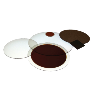
 Fa'aputuga o le silicon dioxide vs. tuputupu a'e
Mo nisi fa'amatalaga e uiga i le fa'aputuina o le ausa vaila'au pe e te mana'o e talosaga mo se tau, fa'amolemoleFESOOTAI I LE SVMi le asō e talanoa ai ma se tasi o la matou 'au fa'atau.
Ituaiga o CVD
LPCVD
O le fa'aputuina o le ausa kemikolo maualalo le mamafa o se faiga masani o le fa'aputuina o le ausa kemikolo e aunoa ma le fa'aputuina o le mamafa. O le eseesega tele i le va o le LPCVD ma isi metotia CVD o le vevela o le fa'aputuina. E fa'aaoga e le LPCVD le vevela aupito maualuga e fa'aputu ai ata tifaga, e masani lava i luga atu o le 600°C.
O le siosiomaga maualalo le mamafa e fausia ai se ata tifaga e matua tutusa lava ma le maualuga o le mama, mafai ona toe gaosia, ma le tutusa. E faia lea mea i le va o le 10 – 1,000 Pa, ae o le mamafa masani o le potu e 101,325 Pa. O le vevela e fuafua ai le mafiafia ma le mama o nei ata tifaga, faatasi ai ma le maualuga o le vevela e mafua ai ni ata tifaga mafiafia ma sili atu ona mama.
- Ata tifaga masani ua teuina:polisilikona, oxides ua fa'aopoopoina ma le le'i fa'aopoopoina,nitrides.
PECVD
O le fa'aputuga o le ausa kemikolo fa'amalosia i le plasma o se metotia fa'aputuga maualalo le vevela ma maualuga le mafiafia o le ata tifaga. E faia le PECVD i totonu o se reactor CVD fa'atasi ai ma le fa'aopoopoina o le plasma, o se kesi fa'aionisi vaega ma le maualuga o le aofa'i o electron saoloto (~50%). O se metotia fa'aputuga maualalo le vevela lea e faia i le va o le 100°C – 400°C. E mafai ona faia le PECVD i le vevela maualalo ona o le malosi mai electrons saoloto e fa'ate'a'eseina ai kesi tali atu e fausia ai se ata tifaga i luga o le fogā'ele'ele wafer.
O lenei metotia o le teuina e faʻaaogaina ai ituaiga plasma se lua:
- Malulu (e lē fa'avevela): e maualuga atu le vevela o eletise nai lo vaega ma ion e le fa'a'autu. O lenei metotia e fa'aaogaina ai le malosi o eletise e ala i le suia o le mamafa i totonu o le potu e teu ai.
- Vevela: e tutusa le vevela o eletise ma vaega ma ions i totonu o le potu e teu ai.
I totonu o le potu e teu ai, e auina atu ai le eletise i le va o eletise i luga ma lalo o le wafer. O lenei mea e faʻatumu ai eletise ma taofia ai i latou i se tulaga e mafai ona faʻaosofia ina ia mafai ona teu ai le ata tifaga e manaʻomia.
E fa laasaga e faʻatino ai le faʻatupulaia o ata tifaga e ala i le PECVD:
- Tuu le target wafer i luga o se electrode i totonu o le potu e teu ai.
- Fa'aofi kasa tali atu ma elemene fa'aputu i totonu o le potu.
- Auina atu le plasma i le va o electrodes ma faʻaaoga le voltage e faʻaosofia ai le plasma.
- E vavae'ese ma tali atu le kasa tali atu ma le fogā'ele'ele o le wafer e fausia ai se ata manifinifi, ae sosolo ese atu oloa e maua mai i fafo o le potu.
- Ata masani e teuina: silicon oxides, silicon nitride, amorphous silicon,silicon oxynitrides (SixOyNz).
APCVD
O le fa'aputuga o le ausa kemikolo i le mamafa o le ea o se metotia fa'aputuga maualalo i le vevela e faia i totonu o se ogaumu i le mamafa masani o le ea. E pei o isi metotia CVD, e mana'omia e le APCVD se kesi muamua i totonu o le potu fa'aputuga, ona si'itia malie lea o le vevela e fa'atino ai tali i luga o le fogā'ele'ele ma fa'aputu ai se ata manifinifi. Ona o le faigofie o lenei metotia, e maualuga tele lona fua faatatau o le fa'aputuga.
- O ata tifaga masani e teuina: silicon oxides ua fa'apipi'iina ma le le'i fa'apipi'iina, silicon nitrides. E fa'aaogaina fo'i i totonufa'amafanafana.
HDP CVD
O le fa'aputuga o le ausa kemikolo plasma maualuga o se fa'aliliuga o le PECVD e fa'aogaina ai se plasma maualuga atu le mafiafia, lea e mafai ai e wafers ona tali atu i se vevela maualalo ifo (i le va o le 80°C-150°C) i totonu o le potu fa'aputuga. O lenei mea e fatuina ai fo'i se ata tifaga e tele ona gafatia e fa'atumu ai le lua.
- Ata masani e teuina: silicon dioxide (SiO2), silicon nitride (Si3N4),silicon carbide (SiC).
SACVD
E ese le fa'aputuga o le ausa kemikolo i le mamafa o le subatmospheric mai isi metotia ona e faia i lalo ifo o le mamafa masani o le potu ma fa'aaoga ai le ozone (O3) e fesoasoani e fa'atino le tali atu. O le fa'agasologa o le fa'aputuga e faia i se mamafa maualuga atu nai lo le LPCVD ae maualalo ifo nai lo le APCVD, i le va o le 13,300 Pa ma le 80,000 Pa. O ata tifaga SACVD e maualuga le fua faatatau o le fa'aputuga ma e fa'aleleia atili pe a fa'ateleina le vevela se'ia o'o i le 490°C, ona amata loa lea ona fa'aitiitia.
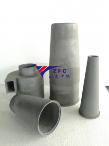
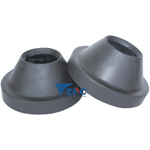
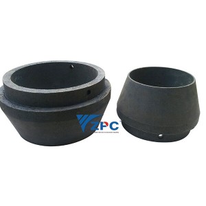
O le Shandong Zhongpeng Special Ceramics Co., Ltd o se tasi o fofo sili ona tele mo mea fou o le silicon carbide ceramic i Saina. SiC technical ceramics: O le malosi o le Moh e 9 (o le malosi o le Moh fou e 13), faatasi ai ma le tete'e lelei i le solo ma le ele, tete'e lelei i le olo ma le tete'e i le okesene. O le umi o le tautua a le oloa SiC e 4 i le 5 taimi e umi atu nai lo le 92% o le alumina. O le MOR o le RBSiC e 5 i le 7 taimi nai lo le SNBSC, e mafai ona fa'aaogaina mo foliga e sili atu ona faigata. O le faiga o le tauofoga e vave, o le tu'uina atu e pei ona folafolaina ma o le lelei e le mafaatusalia. Matou te tumau pea i le lu'itauina o a matou sini ma toe avatu o matou loto i le sosaiete.