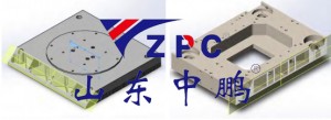
In lithography machines for chip manufacturing, an invisible error can destroy wafers worth millions of dollars. Every micrometer of displacement here is crucial to the success or failure of nanoscale circuits, and the core that supports this precision dance is our protagonist today: silicon carbide ceramic material – it is like a stabilizing force in the microscopic world, guarding the precision lifeline of modern semiconductor industry in extreme environments.
1、 When Ceramics Meet Chips: A Ultimate Challenge in Accuracy
The precision ceramic components of lithography machines need to play three roles simultaneously:
Ultra stable base: withstands several tons of pressure at the moment of exposure but remains motionless.
Temperature sentinel: maintains thermal stability under high thermal shock of laser.
Vacuum Guardian: maintains atomic level flatness for ten years in a zero vibration environment.
Traditional metal materials will produce “micro tremors” due to thermal expansion and contraction, while polymer materials are difficult to resist plasma corrosion. Silicon carbide ceramics, with their unique crystal structure, achieve a perfect balance in hardness, thermal conductivity, and deformation resistance, making them the top choice for the core components of lithography machines.
2、 Nano level precision ‘invisible bodyguard’
In top tier lithography machines such as ASML in the Netherlands, NIKON and CANON in Japan, silicon carbide ceramics are quietly rewriting the rules of precision manufacturing:
Mask stage: carrying a photomask worth as much as gold, maintaining nanometer level positioning accuracy during high-speed movement.
Reflective mirror substrate: The surface roughness is extremely small, even smoother than a mirror surface.
Vacuum chamber: After ten years of use, the deformation is less than one thousandth of a human hair
This almost ‘anti common sense’ stability stems from the triple genes of silicon carbide materials:
1. The coefficient of thermal expansion approaches zero: almost “frozen age” from -150 ℃ to 500 ℃
2. Three times harder than steel: resistant to microscopic damage caused by particle bombardment
3. Self lubrication characteristics: Achieve oil-free precise transmission in a vacuum environment
3、 The ‘silent revolution’ in the semiconductor industry
As the chip manufacturing process enters the 2-nanometer era, silicon carbide ceramics are breaking through more limits:
Dual worktable: allows two systems to complete “atomic level relay” in a vacuum environment.
EUV optical path system: resistant to continuous bombardment of 13.5nm extreme ultraviolet light.
Multi axis linkage system: achieving 200 nanoscale steps per second without generating cumulative errors.
A certain lithography machine R&D team has conducted comparative tests: after using a silicon carbide ceramic workpiece stage, the system positioning accuracy has been improved by 40%, and the equipment maintenance cycle has been extended from 3 months to 2 years. This change not only reduces the production cost of chips, but also brings the manufacturing accuracy of “Chinese chips” to the forefront of international standards for the first time.

4、 The climbing path from laboratory to industrialization
Manufacturing lithography grade silicon carbide ceramics is like building a ‘flawless palace’ in the microscopic world:
Raw material purity: Ultra pure silicon carbide powder, thousands of times purer than edible salt.
Sintering process: precise control of crystal growth direction at high temperatures.
Precision machining using diamond cutting tools for sub micron level carving takes as much time as cultural relic restoration.
It is this dual breakthrough of “materials science+precision manufacturing” that has made cutting-edge materials, which were once limited to aerospace and military industries, now become the fundamental components supporting digital civilization.
In today’s chip manufacturing process, which has reached the physical limit, silicon carbide ceramics prove with its “zero compromise” characteristics that true precision is not the stacking of data, but the ultimate control over the essence of materials. When every ceramic component carries the promise of millions of nanoscale movements, what we see is not only the evolution of semiconductor equipment, but also the determination of a nation’s industry to move towards the peak of precision.
Post time: Apr-03-2025